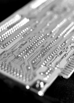
Semiconductor protection secures the rights to three-dimensional structures (topographies) of multi-layered microelectronic semiconductors. A number of nations worldwide, including Germany, offer legal protection of semiconductors.
As a means of protecting your development efforts from copying, and thus safeguarding your business interests, semiconductor protection represents an important and effective instrument in the context of industrial property rights.
In close cooperation with you, we develop concepts for drawing up the required material to identify and illustrate the semiconductor innovations to be protected. In addition, we act as your representatives in conducting registration procedures as well as cancellation procedures before the German Patent and Trademark Office.